Oct 2026· International Symposium for Testing and Failure Analysis· 0 citations
Abstract
The increasing demand for compute power is pushing system scaling toward advanced 3D and backside-integrated architectures. While the wafer backside opens a dynamic design space with new opportunities to optimize power delivery in scaled systems, it also introduces significant challenges for failure analysis (FA). In particular, the application of traditional backside optical fault isolation techniques, widely used for decades, becomes increasingly limited at current leading-edge nodes. As a result, a variety of alternative fault-isolation techniques, including X-ray, thermal, magnetic, and electron-beam approaches, are actively used and developed. Among these, magnetic-field-based techniques enable non-invasive access to buried current paths and connectivity defects, owing to the ability of magnetic fields to propagate through insulators, semiconductors, and metals with minimal disturbance. Early implementations of magnetic field imaging in FA predominantly relied on scanning-probe approaches based on SQUID and GMR sensors. More recently, however, quantum diamond microscopy (QDM) based on nitrogen-vacancy (NV) color centers has gained significant attention, as it enables quantitative current imaging through vector magnetic-field measurements with full-field, parallel, camera-based readout.
Failure analysis (FA) of advanced semiconductor packages is increasingly constrained by the inability of established techniques to image faults buried inside 2.5D and 3D integrated devices. Magnetic current imaging offers a non-destructive route to localising buried currents through opaque packaging, but no existing...
Samuel Mondberg, Luis D. Bonavena, T. K. Pfau et al.· International Symposium for...· 0 citations
Due to progressing miniaturization, material fatigue is expected to gain importance on microscopic scales. Nevertheless, most non-destructive testing techniques are optimized for macroscopic scales. Therefore, new approaches applicable to miniaturized samples need to be explored. High spatial resolution imaging of a ma...
N. Mathes, M. Feuerhelm, S. Philipp et al.· 0 citations
As semiconductor devices continue to scale in complexity and dimensionality, conventional analytical techniques such as SEM-EDS increasingly fall short in providing the spatial resolution and chemical sensitivity required for advanced failure analysis. Deeply buried interfaces, three-dimensional architectures, and ul...
P. Gnauck, Alexander D. Ost, Torsten Richter· International Symposium for...· 0 citations
Quantum diamond microscope (QDM) instruments are an emerging technique being used for high-resolution magnetic field imaging (MFI) applications in a broad range of applications, including geology, biology, condensed-matter physics, and microelectronics. For microelectronics inspection and failure analysis (FA), MFI m...
P. Kehayias, F. Benito, M. Gold et al.· International Symposium for...· 0 citations
The adoption of backside power delivery (BPD) for advanced semiconductor integrated circuit (IC) chips introduces significant electrical fault isolation (EFI) challenges. The lack of direct optical access to the device's FET layer severely impacts techniques such as laser voltage probing and imaging (collectively, LV...
Shaleen Acharya, Manish Sharma, Jayant D'Souza et al.· International Symposium for...· 0 citations
Reconstructing electrical current flow within integrated circuits is a powerful capability for electrical failure analysis (EFA), as it reveals the actual conduction paths associated with defects. Quantum Diamond Microscopy (QDM) enables non-destructive, vector-resolved magnetic field imaging, providing the basis for...
Simon Wanninger, Jin-Cheng Zhang, Maximilian Hecker et al.· International Symposium for...· 0 citations
Related blog posts
Microsoft Research Blog· microsoft.comOct 21, 2026
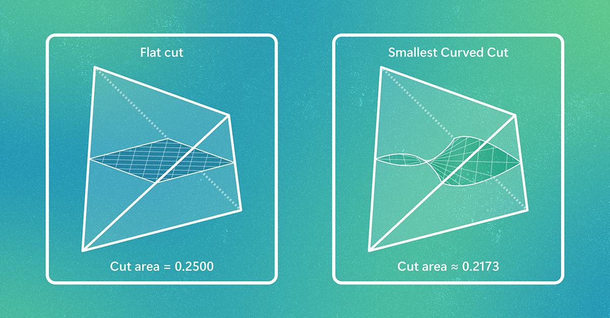
For decades, a fundamental question about the difficulty of computing in high-dimensional spaces has resisted proof. New research resolves this question, removing a major theoretical obstacle to understanding the efficiency of randomized algorithms used across science and computing. The Kannan–Lovász–Simonovits (KLS) conjecture was proposed in 1995. It asks whether, for a broad class of high-dimensional […] The post Solving a 31-year-old grand challenge in mathematics – the KLS conjecture appear…
MIT News · Artificial Intelligence· news.mit.eduOct 15, 2026
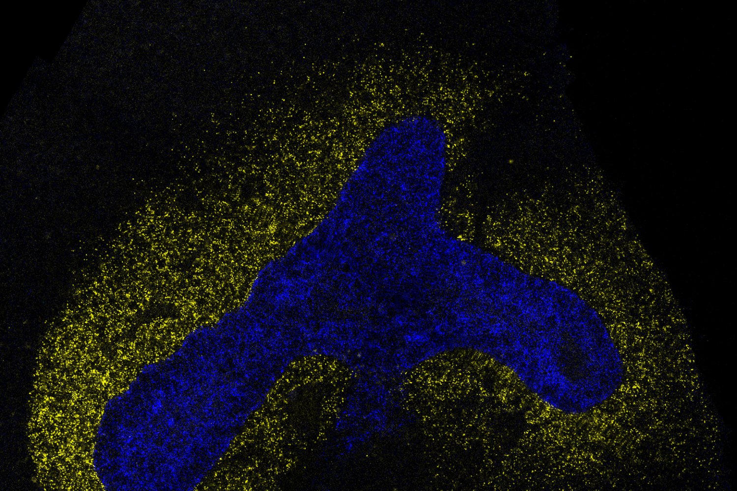
A new computational approach reveals how cells communicate to assemble into tissues. This could accelerate stem cell engineering, improve disease models, and inform therapies.
Microsoft Research Blog· microsoft.comOct 15, 2026
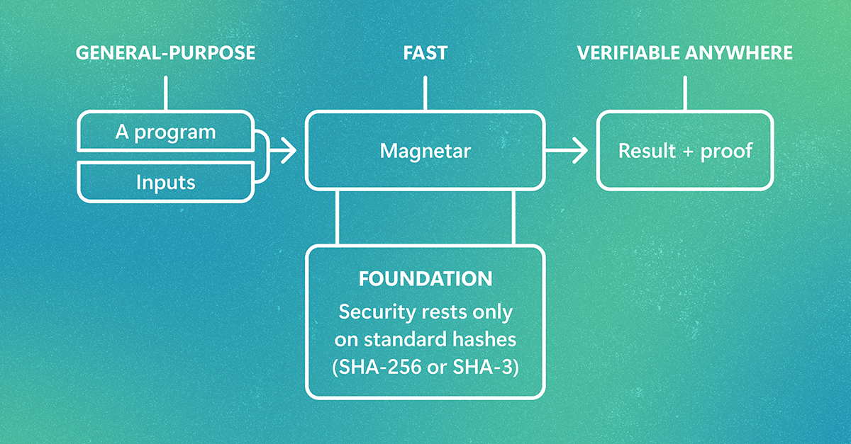
Zero-knowledge proofs can verify computing results without rerunning workloads or exposing sensitive data. Magnetar helps bring them into the mainstream with support for standard programming languages, major speed gains, and quantum-resistant security. The post Proof-based general-purpose computing with Magnetar appeared first on Microsoft Research.
MIT News · Artificial Intelligence· news.mit.eduOct 8, 2026